Metal oxide / Chalcogenide Nano material synthesis& TFT device fabrication by Solution process...
- aeml4735
- Jun 9, 2021
- 1 min read
Updated: Jul 26, 2021
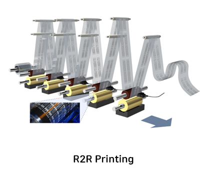
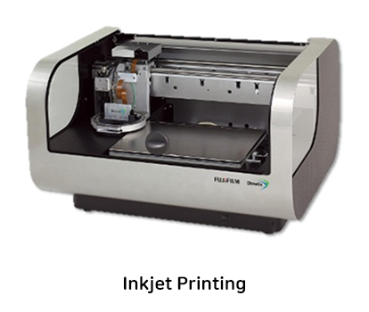
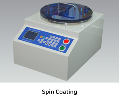
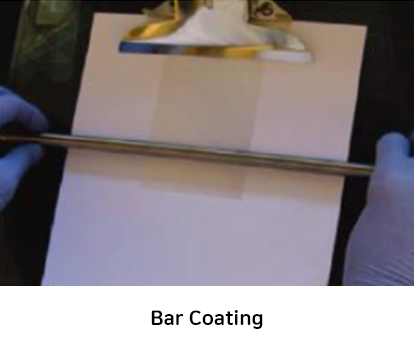
Low temperature solution process has many advantages ; No need vacuum, cost efficiency, mass production, can use flexible substrate. Developing nano materials for semiconductor ink to lowering fabrication temperature. Synthesizing Metal oxide NPs, Telluride NWs & Developing dispersion method for Semiconductor inks. Coating on substrate & making TFT Devices(Spin coating, Bar coating, Inkjet printing, R2R printing) Measuring Electrical property & Surface morphology of active layer.
Metal oxide / Chalcogenide Nano material synthesis & TFT device fabrication by Solution process / Printed electronics
Printed Electronics


Material synthesis & Ink making
- Hydrothermal / Solvothermal
- Heating synthesis
Nanoparticle
Nanowire/rod


Active layer Coating / Printing


Device quality / Performance


Comments